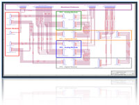
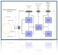
The Plasma Probe's core elctronics are made up of two Analog Modules, two Digital Modules and one Power Module. The electronics interface with four large gold-plated surfaces that form the collector surfaces which detects the plasma particles. Figure to the right provides an electrical block diagram overview.
- Power Module (PM): The principal function of the PM is to provide the analog and digital modules with their required voltages and currents with minimal output jitter.
- Analog Module (AM): The AM comprises mainly the electronics that translates the densities of the plasma particlues to a voltage that can be measured and quantified.
- Digital Module (DM): The DM houses the microcontrollers, the communication circuitry, the ADCs etc. essentially forming the brain of the entire system.
|
 |
Several other supporting hardware and software are required for the functioning of the Plasma Probe. The major supporting components are as follows:
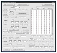
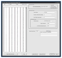
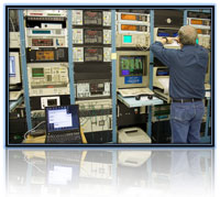
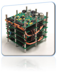
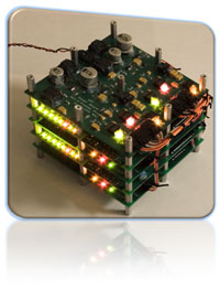
Two pictures of the complete electronics are shown to right.There are a total of five circuit boards; two AMs, two for DM and one for PM (the Power PCB has two separate PM channels built into it). From top to bottom, the first (top most) PCB is the PM, it is followed by the DM1, then by AM1, then by DM2 and AM2, respectively. The completed electronics is mounted into an aluminum enclosure for EMI shielding. The aluminum enclosure is then mounted on to the rocket deck plate to provide by employing conolite fiberglass, which provides thermal isolation from the heavily heated exterior skin of the rocket during flight.
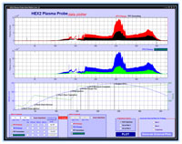
The instrument’s noise resilience is extremely good and it can measure plasma currents as low as 5 nA and with 420 pA resolution. |
 |
 |